How to Optimize Board Level Shielding for EMI Reduction

How to Optimize Board Level Shielding for EMI Reduction
Board level shielding is one of the most targeted tools for controlling electromagnetic interference at the source. Done well, it contains radiated emissions before they couple to neighboring traces, cables, or adjacent boards. Done poorly, it adds cost without changing the result. The difference almost always comes down to a handful of decisions made early in the design process.
What Is Board Level Shielding – and Why Does It Matter?
Board level shielding consists of conductive metal enclosures that mount directly onto a PCB to physically contain electromagnetic interference at the component level. Unlike layout-based techniques – ground planes, trace spacing, copper pours – a metal shield creates a physical barrier around the noise source itself.
Other mitigation methods handle specific parts of the problem. Ferrite beads filter conducted EMI across limited frequency bands. Decoupling capacitors suppress power rail noise locally. These tools are valuable, but they don't contain radiated fields the way a physical shield does. EMI & RFI board level shielding is one of the few techniques that addresses radiation at its origin – not downstream after the noise has already spread.

Why Do Shielded Boards Still Fail EMC Testing?
The most common reason is grounding. A shield that contacts the PCB ground plane only at corners – or with inconsistent force – creates gaps that behave like slot antennas. The shield reflects energy back into the cavity and re-radiates it through every opening available.
Thermal management is another factor that gets underestimated. Metal shields trap heat. Component temperatures rise, operating parameters shift, and EMI generation gets worse – not better. Ventilation geometry and material selection need to account for thermal dissipation, especially in high-power designs.
Key Factors That Determine Shielding Performance
Getting board level shielding right means controlling a small set of variables that have an outsized impact on results. Material choice, aperture sizing, and board compartmentalization each determine whether the shield actually performs to spec.
How to Choose the Right Shielding Material
Not all metals shield equally. Performance differences become significant above 1 GHz, which is where most modern wireless standards operate.
| Material | Conductivity | Cost | Best For |
|---|---|---|---|
| Copper | Very High | High | Broadband, RF-sensitive designs |
| Nickel-Silver | Moderate | Medium | Two-piece snap-on shields |
| Tin-plated Steel | Low–Moderate | Low | Consumer electronics |
| Stainless Steel | Low | Low | General-purpose, cost-sensitive |
Copper is the strongest performer across frequency, but it's also the most expensive. For designs operating below 3 GHz with tight budget constraints, tin-plated steel is a reasonable trade-off. For 5G modules or mmWave radar boards, copper or nickel-silver is the practical minimum.
Aperture Sizing: The Detail That Quietly Kills Shielding Effectiveness
Any opening in a shield – a seam, a vent hole, a connector cutout – reduces shielding effectiveness. The engineering rule is straightforward:
Note: An aperture becomes a significant EMI leak when its longest dimension reaches λ/20 of the highest frequency of concern.
At 5 GHz, that threshold is roughly 3 mm. At 10 GHz, it drops to approximately 1.5 mm. Designs that look solid in CAD often fail this check in production, where tolerance stack-up between the shield wall and the PCB ground pad creates unintended gaps.
Designing for consistent contact force – not just contact – is what determines whether shielding effectiveness holds up across production tolerances.
Multi-Section Shielding for Mixed-Signal Boards
Single-can shielding covers the whole board but does nothing about internal coupling between RF and digital sections. A noisy microcontroller sitting next to an RF front-end inside the same shield enclosure can degrade receiver sensitivity significantly.
The solution is compartmentalization: internal walls connected to the ground plane divide the shield into isolated sections. This approach is standard in telecommunications hardware, automotive control modules, and medical devices – anywhere that EMI & RFI board level shielding must handle both radiated emissions and susceptibility at the same time.
How to Validate Board Level Shielding Performance
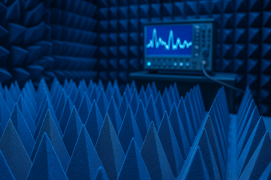
Optimizing board level shielding on the bench is only half the work. The other half is confirming that the shielding actually performs as intended – and that requires a test environment that doesn't introduce its own variables.
A chamber with inadequate absorption produces unreliable data. Reflections off the walls corrupt emission measurements, creating false peaks and masking real ones. Engineering teams end up chasing artifacts instead of actual design problems – which is expensive and time-consuming.
What Makes an EMC Test Environment Reliable
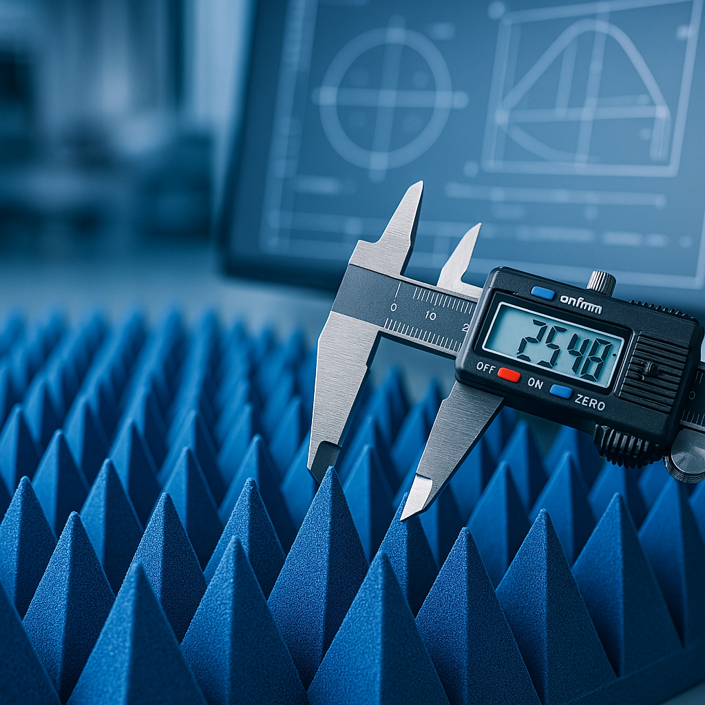
Chambers lined with pyramidal RF absorbers eliminate wall reflections and produce repeatable, accurate results. The absorbers convert incident electromagnetic energy into heat rather than reflecting it back into the measurement space. As covered in anechoic chamber design principles, absorber placement and pyramid sizing relative to wavelength are the two variables that determine whether a chamber produces valid data.

Pre-Submission Checklist: Before Sending a Design to EMC Testing
Before submitting a design for formal testing, verify each of the following:
- Grounding continuity – Shield contacts the PCB ground plane at multiple points around the full perimeter, not just at corners
- Aperture sizing – No slot, seam, or cutout exceeds λ/20 at the highest frequency of concern
- Thermal management – Ventilation geometry is accounted for; component temps under the shield stay within spec
- Section isolation – Mixed-signal boards use compartmentalized shielding to separate RF and digital sections
- Cavity resonance – Designs above 1 GHz have been evaluated for resonant modes; absorber inserts added if needed
- Test environment – Pre-compliance testing runs in a chamber with validated absorber coverage
Make Your EMC Testing Environment Work for You
The work put into optimizing board level shielding is only as reliable as the environment it's tested in. A chamber with poor absorption produces noisy data and wastes engineering time chasing measurement artifacts.
dB Absorber supplies high-performance pyramidal RF absorbers for anechoic chambers and shielded enclosures — with broadband coverage from below 1 GHz through the millimeter-wave range. Whether the goal is a full chamber installation or a compact enclosure retrofit, the product range covers both.
Frequently Asked Questions
Does board level shielding require modifying the PCB layout?
Not significantly. Two-piece and single-piece shields attach via a soldered fence on the PCB ground plane. The layout impact is minimal, but the ground pad perimeter needs to be planned during the design phase – it's difficult to add cleanly after the fact.
What frequency range does board level shielding cover?
Metal shields are effective from near-DC through tens of gigahertz, depending on material and construction quality. Above 1 GHz, material conductivity and aperture control become the limiting factors. For millimeter-wave designs (above 30 GHz), the test environment needs to match – standard Faraday enclosures without proper absorber lining produce unreliable results at those frequencies.
What is the difference between single-piece and two-piece board level shielding?
A single-piece shield is soldered directly to the PCB and requires reflow to remove – useful for production but inconvenient for rework. A two-piece design uses a soldered fence and a snap-on lid, which allows access to components underneath without desoldering. Two-piece shields are the standard choice when in-field access or post-assembly testing is expected.
How does the test chamber affect EMC measurement accuracy?
Directly. A chamber without adequate RF absorption reflects signals back onto the device under test, distorting both radiated emission measurements and immunity results. Pre-compliance testing in a poorly treated enclosure can give false confidence – a board that passes in-house may still fail at an accredited lab if the environments differ significantly.