Millimeter Wave Absorbers for 6G Testing: What Engineers Need to Know in 2025
Meta-description: Explore the role of millimeter wave absorbers in 6G testing, addressing new challenges and materials needed to handle sub-terahertz frequencies in 2025.
Millimeter Wave Absorbers for 6G Testing: What Engineers Need to Know in 2025
The telecommunications world rarely stands still. Even as 5G networks expand globally, the race toward 6G has already begun. This next generation won't just improve existing technology—it demands completely new testing methods and materials that can handle frequencies most labs have never worked with before.
The real challenge? Testing equipment that operates between 100 and 300 GHz, a range known as the sub-terahertz spectrum. Traditional materials that worked fine for 5G suddenly fall short, creating an urgent need for better solutions, such as millimeter wave absorbers, to manage these higher frequencies effectively.
Why Sub-Terahertz Testing Changes Everything
Previous wireless generations operated at relatively manageable frequencies. 5G topped out around 95 GHz, but 6G pushes into 100-300 GHz territory. This isn't just a number bump—the physics fundamentally changes at these higher frequencies.
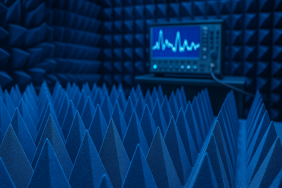
Electromagnetic waves in this range behave unpredictably. They reflect more easily, penetrate materials differently, and require extremely precise control to measure accurately. Testing chambers depend on special absorbing materials, such as millimeter wave absorbers, to eliminate unwanted reflections, but older designs can't handle these new frequencies.
There's also a problem called "self-poisoning." When noise from inside a device bounces off surrounding surfaces instead of being absorbed, it interferes with the device's own operation. Metal shielding that blocks lower frequencies actually makes things worse by reflecting sub-terahertz waves even more aggressively.
Breaking Free from Old-School Absorber Designs
Traditional electromagnetic absorbers relied on a simple trick: they worked alongside metal backing plates, canceling out waves through phase interference. This worked well enough for older wireless tech, but fails completely for 6G applications.
Recent breakthroughs have produced materials that absorb 70% or more of electromagnetic waves across the entire 100-300 GHz range. Some advanced versions hit 80% absorption at 140 GHz, a frequency particularly relevant for 6G development. These numbers represent serious progress given the technical hurdles involved.
The Liquid Solution That's Changing the Game
The biggest innovation? Liquid formulations that cure with heat. Unlike rigid sheets that dominated earlier generations, these liquid materials can be applied exactly where needed. They conform to irregular surfaces, solving a longstanding headache for chamber designers who deal with complex geometries and awkward corners.
These new materials use specialty fillers combined with engineered polymer matrices—far more sophisticated than the carbon-loaded foams of the past. The flexibility matters because real testing environments rarely feature simple flat walls. Equipment, fixtures, and structural necessities create countless angles that traditional sheet absorbers, including millimeter wave absorbers, struggle to cover properly.
What Performance Actually Matters for 6G Testing
Engineers testing 6G systems need absorbers that handle specific technical requirements. Getting these wrong means unreliable measurements and wasted development time.
Key specifications that make or break testing accuracy:
- Absorption efficiency above 90% to keep reflections below equipment noise floors
- Broadband performance maintaining effectiveness across the full 100-300 GHz spectrum
- Minimal thickness to fit space-constrained chambers without sacrificing performance
- Environmental stability across normal temperature and humidity variations
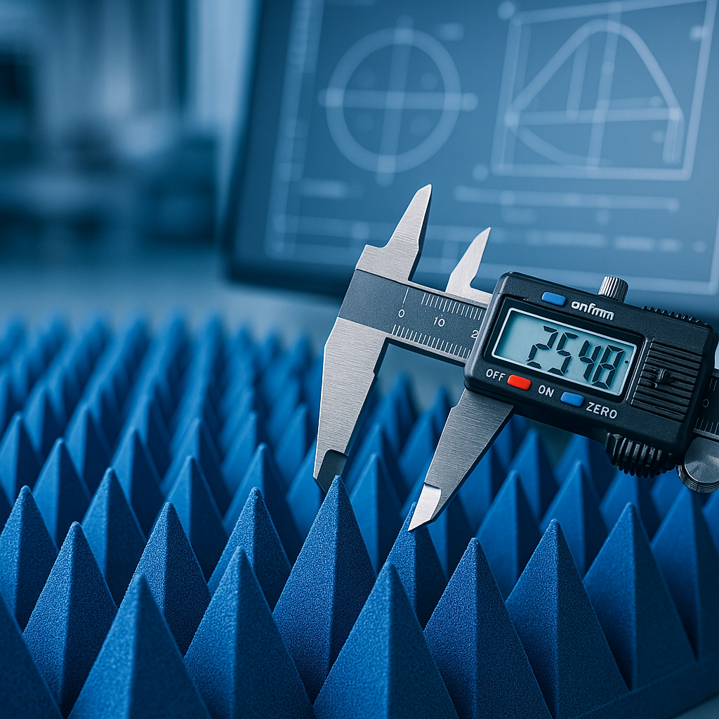
The thickness challenge particularly frustrates facility designers. Ideal absorption might require several inches of material, but many chambers simply don't have that space available. The best absorbers maximize performance while staying compact—a difficult balance requiring sophisticated engineering.
Metamaterials: The Technology That Sounds Like Science Fiction
Perhaps no development excites testing engineers more than metamaterial-based absorbers. These artificially structured materials achieve electromagnetic properties that don't exist in nature, delivering near-perfect absorption in remarkably thin profiles.
The real breakthrough? Digital coding metasurfaces that allow tunable absorption characteristics. A single material can potentially adapt to different frequency bands or operational requirements. For 6G testing, where systems operate across various sub-terahertz frequencies, this flexibility proves invaluable.
Flexible metamaterials solve another common problem: curved or irregular surfaces. Traditional rigid absorbers can't conform to the complex geometries found in modern antenna systems. Recent advances have produced metamaterial designs that maintain absorption properties even when bent or shaped.
When Heat Becomes the Hidden Enemy
Higher frequencies mean higher power densities. As electromagnetic energy gets absorbed, it converts to heat. In confined testing spaces with limited airflow, this heat buildup causes real problems.
A millimeter wave absorber must withstand elevated temperatures without degrading. But thermal performance goes beyond just surviving heat—materials need reasonable thermal conductivity to dissipate energy rather than creating hot spots. Some developers now explore hybrid designs incorporating thermally conductive fillers, though balancing electromagnetic and thermal performance requires careful trade-offs.
Manufacturing Methods Catching Up to Technology
The convergence of absorber technology with printed electronics could revolutionize production costs. Screen-printable and inkjet-printable formulations have shown absorption efficiencies exceeding 90% at certain frequencies. While these demonstrations haven't covered the full 6G range yet, they suggest potential cost reductions up to 40% compared to traditional manufacturing.
Printed absorbers offer advantages beyond just price. They enable complex patterns and gradual thickness transitions impossible with conventional methods. This design freedom lets engineers optimize absorption profiles for specific chamber geometries or measurement scenarios.
Testing the Testers: Validation Gets Complicated
Measuring absorber performance at sub-terahertz frequencies presents unique difficulties. Not all facilities possess the instrumentation needed to accurately evaluate materials at 100-300 GHz. Standard testing protocols developed for lower frequencies don't translate directly, requiring new methodologies and calibration procedures.
The lack of universal testing standards for novel materials, such as millimeter wave absorbers, creates additional headaches. Different manufacturers might use varying measurement techniques, making direct comparisons nearly impossible. This standardization gap slows adoption as engineers struggle to verify vendor claims.
Current challenges facing absorber validation:
- Missing standardized test procedures for sub-terahertz frequencies
- Limited availability of calibrated measurement equipment
- Inconsistent reporting methods between manufacturers
- Long certification cycles for safety and regulatory compliance
Over-the-Air Testing Becomes Non-Negotiable
At millimeter wave and sub-terahertz frequencies, antennas often integrate directly with other components. This makes traditional testing impractical or outright impossible. Testing must happen over the air, which demands anechoic chambers with extremely high performance standards.
Chamber design becomes critical as frequencies increase. Absorber coverage must be comprehensive, with special attention to edges, corners, and transitions between surfaces. Small gaps or imperfections that wouldn't matter at lower frequencies introduce significant measurement errors in the sub-terahertz range.
AI Steps In Where Human Intuition Falls Short
Artificial intelligence now plays a growing role in both absorber design and test system optimization. Machine learning algorithms analyze vast parameter spaces to identify optimal material compositions or predict performance before physical prototyping. This computational approach accelerates development and sometimes reveals solutions human designers would miss.
In test systems, AI-driven signal analysis helps extract meaningful data from complex 6G waveforms. The combination of advanced materials and intelligent analysis creates testing environments capable of handling sub-terahertz communication demands.
Supply Chain Realities Nobody Talks About
High-performance absorbers require specialized ingredients that aren't commodity products. Rare earth elements and particular carbon compounds face availability constraints and price swings. Geopolitical tensions occasionally disrupt supply lines, with lead times stretching beyond six months during shortages.
Manufacturers have diversified supplier bases and developed alternative formulations, but these measures only partially address the core issue. The most advanced millimeter wave absorber materials need components that simply aren't mass-produced yet.
The Road from Research Lab to Real Networks
As 6G transitions from pure research toward early standardization, demand for sub-terahertz test facilities grows. The market currently serves mainly research institutions and major equipment manufacturers, but this will expand significantly as the technology matures.
Engineers working on 6G systems can't just adapt 5G testing methods and hope for reliable results. The frequency difference demands fundamentally different materials and approaches. Collaboration between system developers and material specialists has become necessary, with both groups needing to understand each other's constraints.
What successful 6G testing requires:
- Purpose-built absorbers validated for 100-300 GHz operation
- Chamber designs optimized for sub-terahertz characteristics
- Updated measurement protocols and calibration standards
- Integration of advanced analysis tools and AI assistance
The technical challenges remain substantial. Achieving consistent absorption across the full 6G band while maintaining reasonable thickness, cost, and environmental resilience demands continued innovation. Yet recent progress shows these obstacles, while significant, can be overcome with focused effort and investment.
Moving Forward
The jump to 6G frequencies represents more than just incremental progress—it's a fundamental shift requiring new materials and testing methodologies. Engineers must move beyond solutions adequate for 5G and work closely with material specialists to develop absorbers specifically validated for the sub-terahertz range. Only through this collaborative approach can testing facilities deliver the accuracy and reliability that next-generation wireless systems demand.
Looking for high-quality RF absorbers? Browse our in-stock pyramidal absorbers — shipping from California in 1-2 business days.